Project Code: PN-III-P2-2.1-PED-2019-2386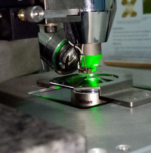
Contract Number: 417PED/2020
Project Title: Integrated writing/imaging platform for nanoscale creation of surface optical waveguides and photonic crystals for optical computing
Duration: 01.11.2020 – 01.11.2022
Grant value: 600 000 Lei (~ 123 000 EURO)
2020 Stage summary
2021 Stage summary
2022 Stage summary
SHORT PRESENTATION OF PROJECT’S RESULTS
Abstract:
The INTEGRAOPTIC project aims to build an integrated optical system of writing/imaging/testing of optical planar waveguides and different types of 2D photonic crystals. These waveguides and photonic crystals will be written on different types of materials (different glasses, polymers, silicon, oxides, etc) by using a technique based on non-linear optical effects which appear when illuminating the material with pulsed femtosecond lasers. As an effect, the refractive index of the materials changes locally. Apart from the commonly used techniques, in INTEGRAOPTIC we will combine the pulsed femtosecond laser writing technique with the “tip-enhancement” effect, which consists in light amplification in the proximity of a nano-probe’s tip. In our project, such nano-probe will be used by our home-made scattering scanning near-field optical microscope (s-SNOM). This combination of the two physical effects will conduct not only to a lower laser power necessary for changing the refractive index, but also to modifications of the refractive index in a small spatial domain (with nanoscale resolution). The imaging unit will be upgraded from the current version, which already contains an s-SNOM, an atomic force microscope (AFM) and a confocal laser scanning microscope (CLSM). The s-SNOM part will be upgraded to allow for in-depth imaging. The testing unit will contain a laser-infection system necessary for injecting the laser beam inside the created optical devices, a particular SNOM version for quality evaluation of the devices during functioning and a CCD camera for evaluation of the output of the optical devices. At the end, the integrated optical system will be capable to build optical devices for optical computing, to image them with nanoscale resolution and to test their quality.
Project objective:
The aim of the project is to develop a technical platform capable of modifying, locally and in a controlled manner, the refractive index at the surface of different optical materials for creation of basic structures of optical surface waveguides and 2D photonic crystals. Moreover, this platform will be capable to image and test these optical structures.
Funding Agency:
Executive Unit for Financing Higher Education, Research, Development and Innovation (UEFISCDI)